
There has been a lot of controversy about this matter in the last days, but we will try to clarify that Playstation 4 supports hUMA technology or at least it implements a first revision of it. We have to remember that AMD haven’t released products with hUMA technology yet, so it is difficult to compare with something in the market. Besides, no finished specifications are settled yet, therefore PS4 implementation may differ a bit with finished hUMA implementations.
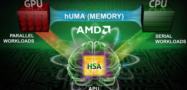
But first of all, what is hUMA? hUMA is the acronym for Heterogeneous Uniform Memory Access. In the case of hUMA both processors no longer distinguish between the CPU and GPU memory areas. Maybe this picture could explain the concept in a easy way:

If you want to learn more about this tech, this article explains how hUMA works.
PS4 has enhancements in the memory architecture that no other “retail” product has, as Mark Cerny pointed in different interviews. We will try to show the new parts in PS4 components in the next pages.
We need to put our diagram about PS4 memory architecture to explain how it works.

Mapping of memory in Liverpool
– Adresses are 40 bit. This size allows pages of memory mapped on both CPU and GPU to have the same virtual address
– Pages of memory are freely set up by the application
– Pages of memory do not need to be both mapped on CPU and GPU
- If only the CPU will use, the GPU does not need to have it mapped
- If only the GPU will use, it will access via Garlic
– If both the CPU and GPU will access the memory page, a determination needs to be made whether the GPU should access it via Onion or Garlic
- If the GPU needs very high bandwidth , the page should be accessed via Garlic; the CPU will need to access it as uncached memory
- If the CPU needs frequent access to the page, it should be mapped as cached memory on the CPU; the GPU will need access it via Onion.
Five Type of Buffers
– System memory buffers that the GPU uses are tagged as one of five memory types
– These first three types have very limited CPU access; primary access is by the GPU
– Read Only (RO)
- A “RO” buffer is memory that is read by CU’s but never written to them, e.g a texture or vertex table
- Access to RO buffers can never cause L1 caches to lose coherency with each other, as it is write operations that cause coherency problems.
– Private (PV)
- A “PV” buffer is private memory read from and written to by a single threadgroup, e.g. a scratch buffer.
- Access to PV buffers can never cause L1 caches to lose coherency, because it is writes to shared memory areas that cause the problems
– GPU coherent (GC)
- A “GC” buffer is memory read from and written to by the CU’s as a result of draw calls or dispatches, e.g. outputs from vertex/shaders that are later read by geometry shaders. Depth buffers and render targets are not GC memory as they are not written to by the CU, but by dedicated hardware in the DBs and CBs.
- As writes are permitted to GC buffers, access to them can cause L1 caches to lose coherency with each other
– The last two types are accessible by both CPU and GPU
– System coherent (SC)
- A “SC” buffer is memory read from and written to by both CPU and GPU, e.g. CPU structure GPU reads, or structures used for CPU-GPU communication
- SC buffers present the largest coherency issues. Not only can L1 caches lose coherency with other, but both L1 and L2 can lose coherency with system memory and the CPU caches.
– Uncached (UC)
- A “UC” buffer is memory that is read from and written to by both CPU and GPU, just as the SC was
- UC buffers are never cached in the GPU L1 or L2, so they present no coherency issues
- UC accesses use the new Onion+ bus, a limited bandwidth bus similar to the Onion bus
- UC accesses may have significant inefficiencies due to repeated reads of the same line, or incremental updates of lines
– The first three types (RO, PV, GC) may also be accessed by the CPU, but care must be taken. For example, when copying a texture to a new location
- The CPU can write the texture data in an uncached fashion, then manually flush the GPU caches. The GPU can then subsequently access the texture as RO memory through Garlic at high speed
- Two dangers are avoided here. As the CPU worte the texture data using uncached writes, no data remains in the CPU caches and the GPU is free to use Garlic rather than Onion. As the CPU flushed the GPU caches after the texture setup, there is no possibility of stale data in the GPU L1 and L2.
Tracking of Type in Memory Accesses
– Memory accesses are made via V# and T# definitions that contain the base address and other parameters of the buffer or texture
– Three bits have been added to V# and T# to specify the memory type
– And extra bit has been added to the L1 tags
- It is set if the line was loaded from either GC or SC memory (as opposed to RO or PV memory)
- A new type of packet-based L1 invalidate has been added that only invalidates the GC and SC lines
- A simple strategy is for application code to use this invalidate before any draw call or dispatch that accesses GC or SC buffers
– An extra bit has been added to the L2 tags
- It indicates if the line was loaded from SC memory
- A new L2 invalidate of just the SC lines has been added
- A new L2 writeback of just the SC lines has been added. These both are packet-based.
- A simple strategy is for application code to use the L2 invalidate before any draw call or dispatch that uses SC buffers, and use the L2 writeback after any draw call or dispatch that uses SC buffers
- The combination of these features allows for efficient acquisition and release of buffers by draw calls and dispatches
Simple Example:
– Let’s take the case where most of the GPU is being used for graphics (vertex shaders, pixel shaders and so on)
– Additionally, let’s say that we have an asynchronous compute dispatch that uses a buffer SC memory for:
- Dispatch inputs, with are created by the CPU and read by the GPU
- Dispatch outputs, which are created by the GPU and read by the CPU
– The GPU can:
1) Acquire the SC buffer by performing an L1 invalidate (GC and SC) and an L2 invalidate (SC lines only). This eliminates the possibility of stale data in the caches. Any SC address encountered will properly go offchip (to either system memory or CPU caches) to fetch the data.
2) Run the compute shader
3) Release the SC buffer by performing an L2 writeback (SC lines only). This writes all dirty bytes back to system memory where the CPU can see them
– The graphics processing is much less impacted by this strategy
- On the R10xx, the complete L2 was flushed, so any data in use by the graphics shaders (e.g. the current textures) would need to be reloaded
- On Liverpool, that RO data stays in place – as does PV and GC data
This technical information can be a bit overwhelming and confuse, therefore we will disclose more information and examples of use of this architecture in a new article this week.
![[Rumor] Rockstar cancelled -for a third time- Bully 2 in 2017](https://vgleaks.com/wp-content/uploads/2013/11/bully-trademark.jpg)


